Fab floor
What actually happens at a wafer probe
Wafer probe is electrical test of dies while they are still on the intact wafer. A probe card presents a field of needles or microsprings to bond pads or bumps. Automatic test equipment runs a program. Each site is binned, the wafer is mapped, and only then does the lot move toward dicing and assembly. The silicon is still one disk.
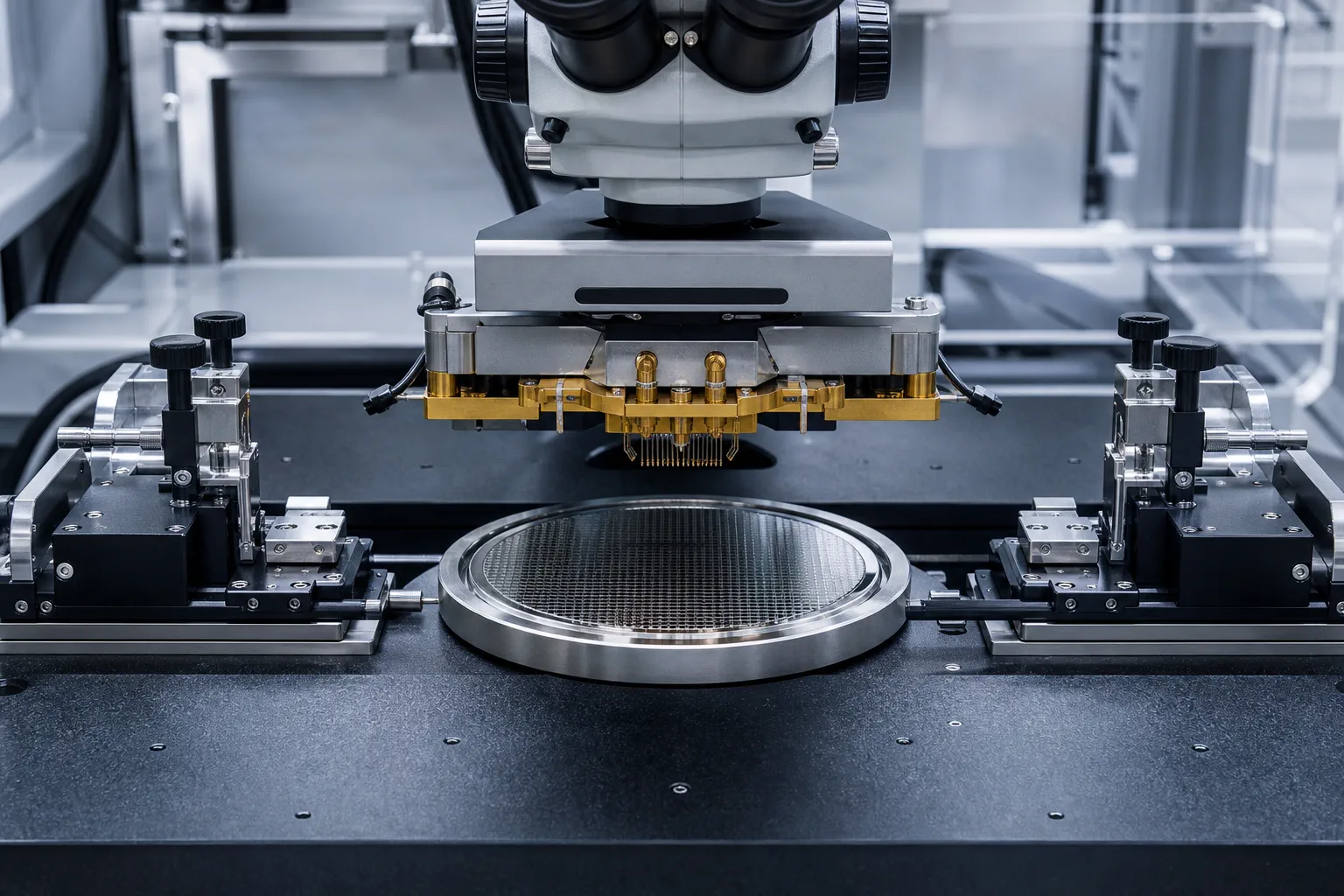
The cell is a precision aligner with a vacuum chuck, not a packaging tool. The wafer sits on the chuck. The card hangs above it. Software walks the stepping grid so every die — or every sampled die — gets a touchdown. Overtravel, planarization, and alignment are mechanical problems. A miss here is a false fail or a damaged pad, not a lithography defect.
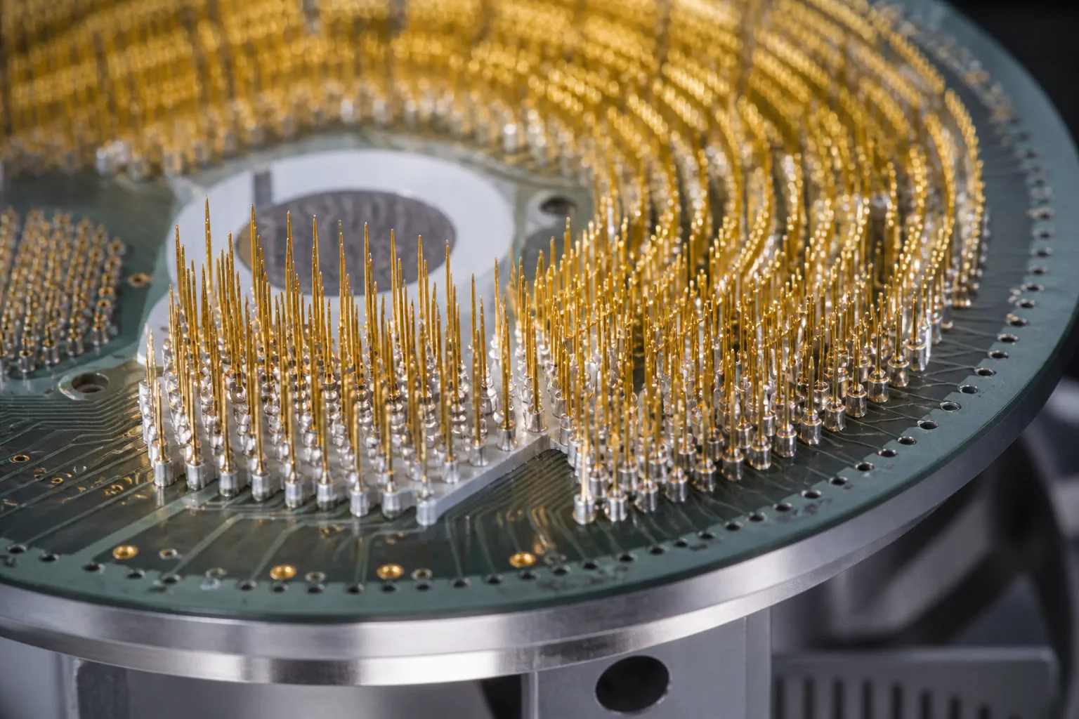
The card is the custom part. A production card is a printed circuit or a ceramic plate with a dense set of tips, each aimed at a pad or a bump. Cantilever, vertical, and MEMS cards differ in compliance and density, but they share a job: land, wipe a little, and leave a mark the next step can live with. A bent tip, a dirty pad, or wrong overtravel shows up in the binning before it shows up in a package.
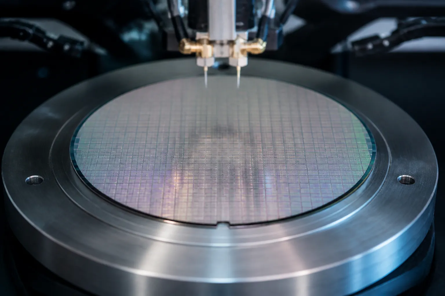
What the tester asks depends on the product and on how expensive a second of cell time is. A parametric insert may measure leakage, threshold, or a monitor structure in the scribe. A functional insert may start a built-in self-test, scan a block, or run a memory march. High-volume logic often runs a reduced pattern set at probe and keeps the long suite for package test. The wafer is still whole. Time on the cell is not.
The chuck can be cold, hot, or both. Some lots see more than one temperature pass. Some products see a fuse or trim in the same visit: measure, blow, measure again. Probe is a gate, and it is sometimes the last station that can still adjust a die before the wafer is cut.
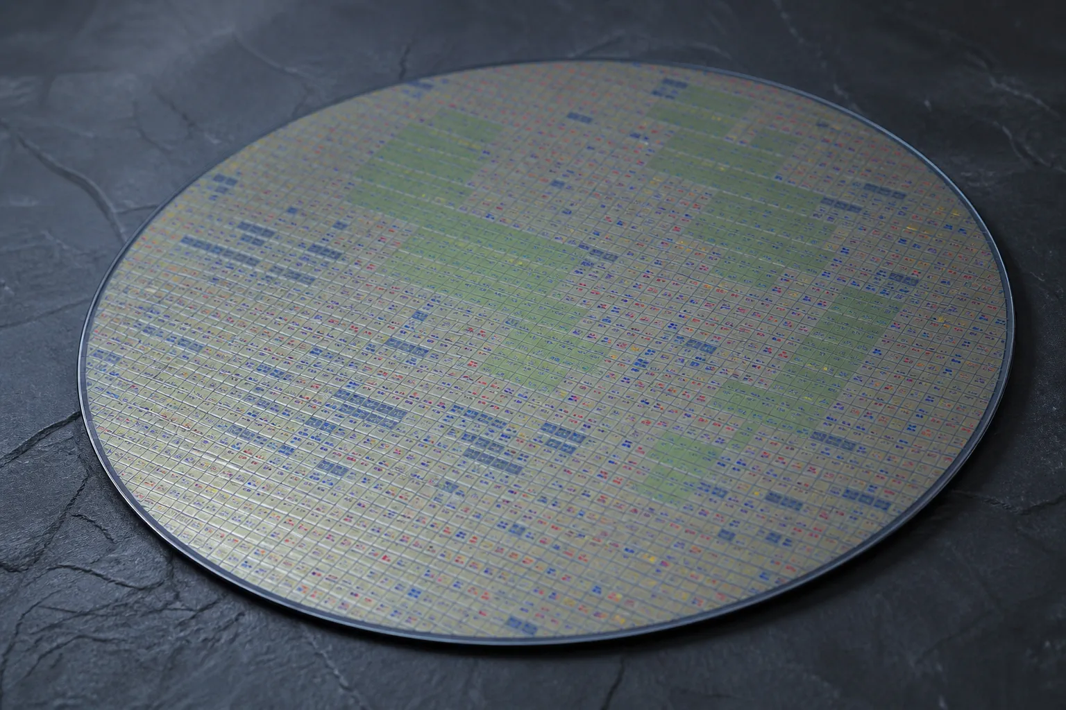
The output that matters to the next boat is the wafer map. Each site gets a bin: good enough for the main product, good enough for a slower bin, reject, or do-not-pick. Ink dots used to mark the bad sites. Most lines now keep an electronic map and let the dicer or pick tool read it. That file is how a bad die is kept out of a good package.
Probe and final test both use a tester and both produce a yield number. They are not the same step. Probe is still on the wafer. Final test is usually after the die is in a package, with different access, different thermals, and a different program. A die can pass probe and fail later. A die can also be rejected at probe for a pad or probe-card issue that would never have appeared in a socket.

The racks beside the station are the automatic test equipment: channels, power supplies, and the computer that runs the program. Cables to the probe card stay short. Extra length is inductance and a chance to fail a timing check the silicon would have passed. When a cell is down, the first suspects are a card, a cable, or a dock, not a mystery in the process recipe.
Sort is the decision, not the needles. After the map is closed, a rule chooses which bins ship to assembly. A colored grid on a wafer, or a file that looks like one, is the record of that decision. It is not a process defect map from a scan tool, and it is not a utilization chart from dispatch. It is a list of sites and scores.
Three facts define the station: what is touching the pads, what program is running, and what map leaves with the lot. Those three answers are wafer probe. Package test, system test, and burn-in are later stations with later access and later programs.