Process
Why a nanometer node is not a transistor size
A foundry node name is a generation label for a process family. It is not a transistor width and not a gate length. When a slide says “3 nanometer,” the integer is a commercial handle for a bundle of density, speed, power, and design rules. It is not a claim that any one feature on the wafer measures three nanometers.
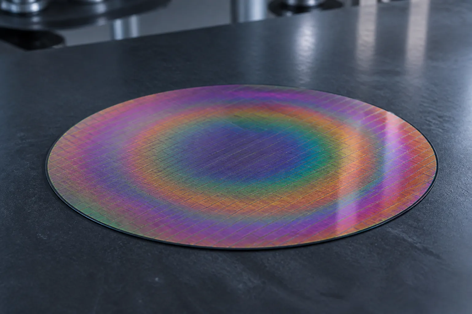
For several early CMOS generations the public number tracked a geometry you could pull from a cross-section or a drawn layer: half-pitch, or a gate length on the reticle. That coupling broke as contacted poly pitch, fin pitch, and interconnect pitch stopped moving in lockstep, and as vendors stopped agreeing on one shared geometric standard. The name stayed. The measurement underneath it did not.
That is why two products sold under the same node integer can disagree on the distances that actually sit in silicon. Contacted poly pitch on one flow can be looser than on another. Minimum metal pitch can differ by layer and by product. An SRAM bit cell can be smaller on the part that looks, on a slide, like the older name. The brochure integers are not a common ruler.
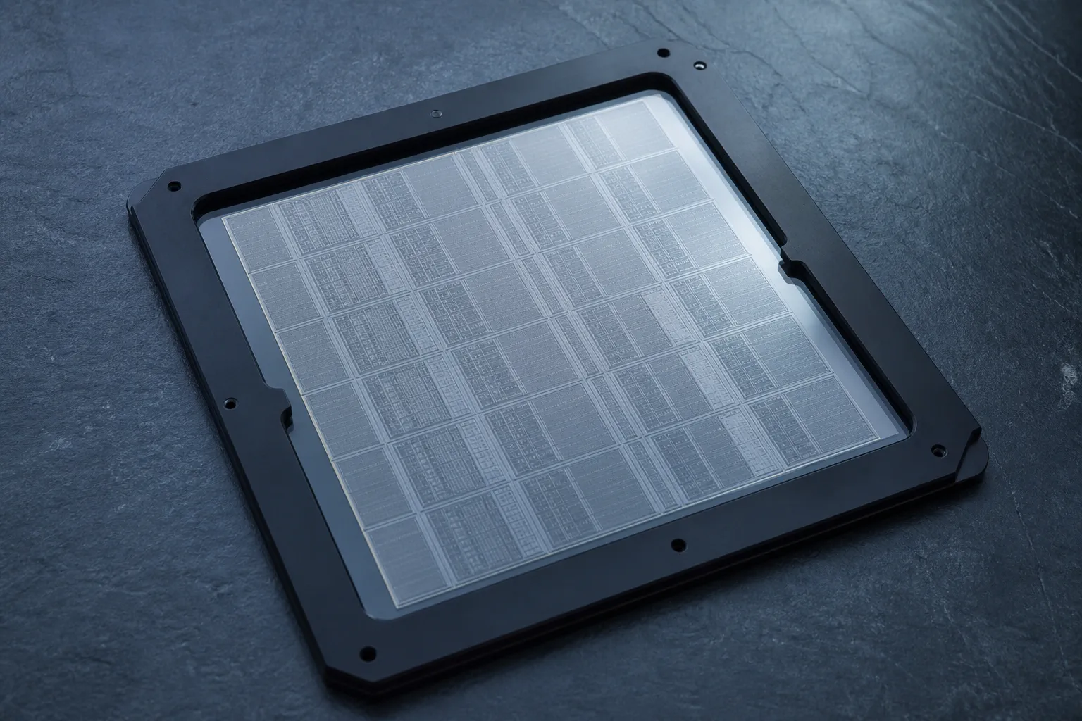
The useful sizes are still ordinary. Contacted poly pitch is the repeat distance of the gate along the cell. Metal pitch is the repeat distance of a given interconnect layer. Fin pitch, or the stack height of a nanosheet device, describes the body of the transistor. Track height in the standard-cell library sets how tightly logic packs. None of those numbers is required to equal the marketing node. A lithography reticle still carries the real drawn shapes. The node name does not have to appear on that glass.
The nanometer persists because the unit is real. Gates, spacers, and lines are measured in nanometers. Putting that unit on a generation name makes the name read as a dimension. A shrink announcement then gets treated as a scale factor — half the size, twice the count — which is not what the label promises. A new node can buy performance with a new device architecture, a new middle-of-line scheme, or a new library, not only with a tighter pitch.
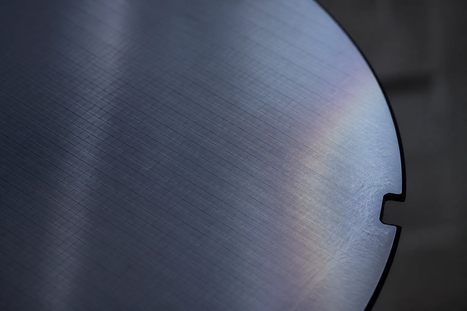
The wafer does not announce the node. Oxide color, notch, and polish say you are looking at silicon. They do not say whether the lot is a “5” or a “3.” That integer lives in the traveler, the process of record, and the press slide. Treating the disk you can hold as proof of the label is the same error as treating a process name as a metrology result.
Die-size work has to go through the library, not the announcement. A standard-cell track height, a contacted poly pitch, and a minimum metal pitch set congestion and dynamic power. Those are the knobs. The node name is the folder those knobs arrived in.
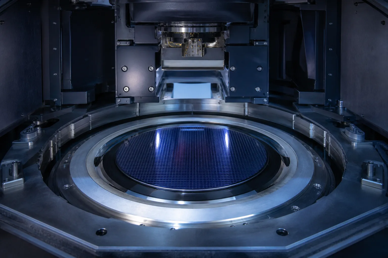
Lithography is a second split. Extreme ultraviolet scanners print a tighter pitch on critical layers than the deep-ultraviolet tools they replaced, but a node is not “the wavelength.” Multi-patterning on an older scanner can still land a pitch that a casual reading would file under a smaller name. The chamber is a printer. The node is the product family that printer is serving on this flow.
Interconnect is a third split. After the device is built, copper lines and vias carry the signal. Those layers have their own pitches, resistance, and capacitance. A small transistor does not make the wiring small. Delay can still be a metal problem. A microscope view of interconnect is a map of wiring, not a proof of the brochure integer.
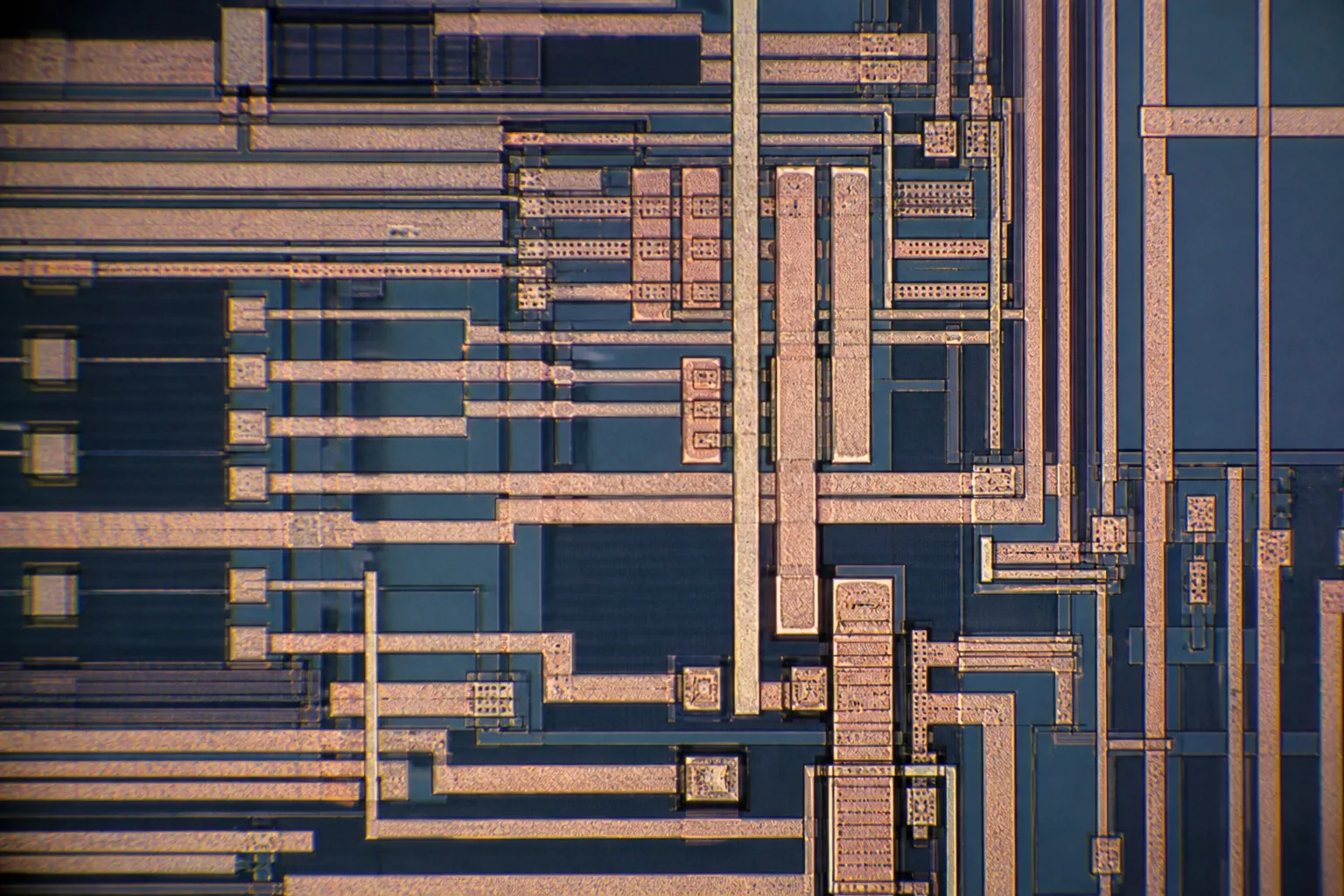
If a physical comparison is required, ask for contacted poly pitch, a published minimum metal pitch, and a density figure such as SRAM cell size or transistors per square millimeter. Those numbers are still marketing-adjacent, and they still vary by product. They at least point at geometry instead of a generation nickname.
Read a node name as a generation label. Read a pitch as a size. When a part is called “3 nanometer,” the open question is which pitch is meant — and whether a pitch is meant at all.