Process
Why overlay is not CD
Critical dimension is a feature size. Overlay is how well this layer sits on the last one. A CD tool asks whether a line, space, or hole on this layer meets the width target. An overlay tool asks whether the new pattern landed where the prior layer said it should. Both results are reported in nanometers. They do not share a meaning.
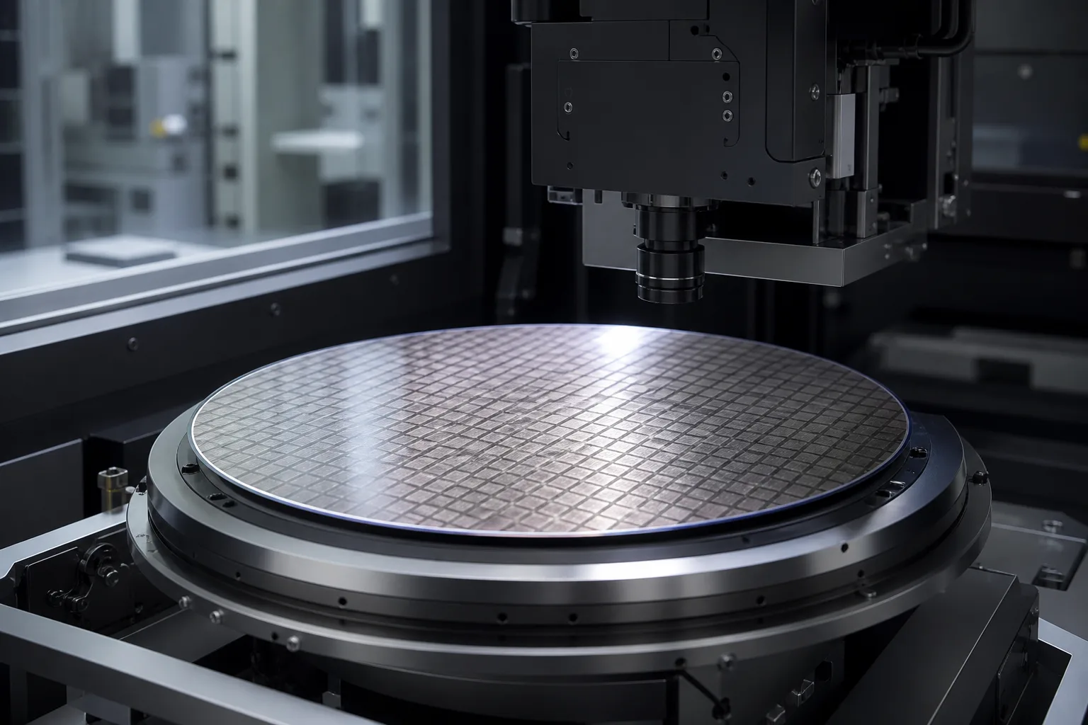
The industry split is old and official. The ITRS lithography chapter lists CD control and overlay as separate requirements: size must hold across the field, the wafer, and the lot; placement must be accurate with respect to underlying layers if the circuit is going to yield. NIST treats the two measurements the same way. A gate that is the right width on a layer that missed the contact is still a miss.
The collapse is easy because both numbers live on a lithography slide and both use the same unit. A scanner brochure quotes overlay as a machine residual — how tightly the tool can put this exposure on a prior mark. That residual is not a gate length and not a metal linewidth. Reading the overlay spec as “how small the transistor is” is the same error as reading a node name as a pitch.
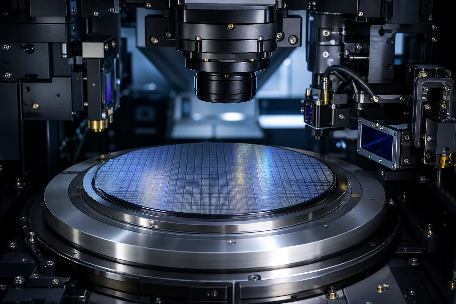
A wafer can pass CD and still be scrap. The lines can be the right size and sit in the wrong place. A contact that does not land on the pad, a via that misses the metal, a cut that shears the wrong line — those are registration failures. The CD-SEM can be green while the overlay map is not. Edge placement is where the two meet: a feature’s edge lands or misses based on both its width and where the layer was printed. Passing one check does not finish the other.
The tools differ. CD is often a CD-SEM or an optical scatterometry recipe on a repeating structure. Overlay is often an optical measurement of a dedicated mark printed in two layers. The scanner also reads alignment marks before it prints. Alignment is the setup. Overlay is the leftover after the exposure. They are related. They are not synonyms.
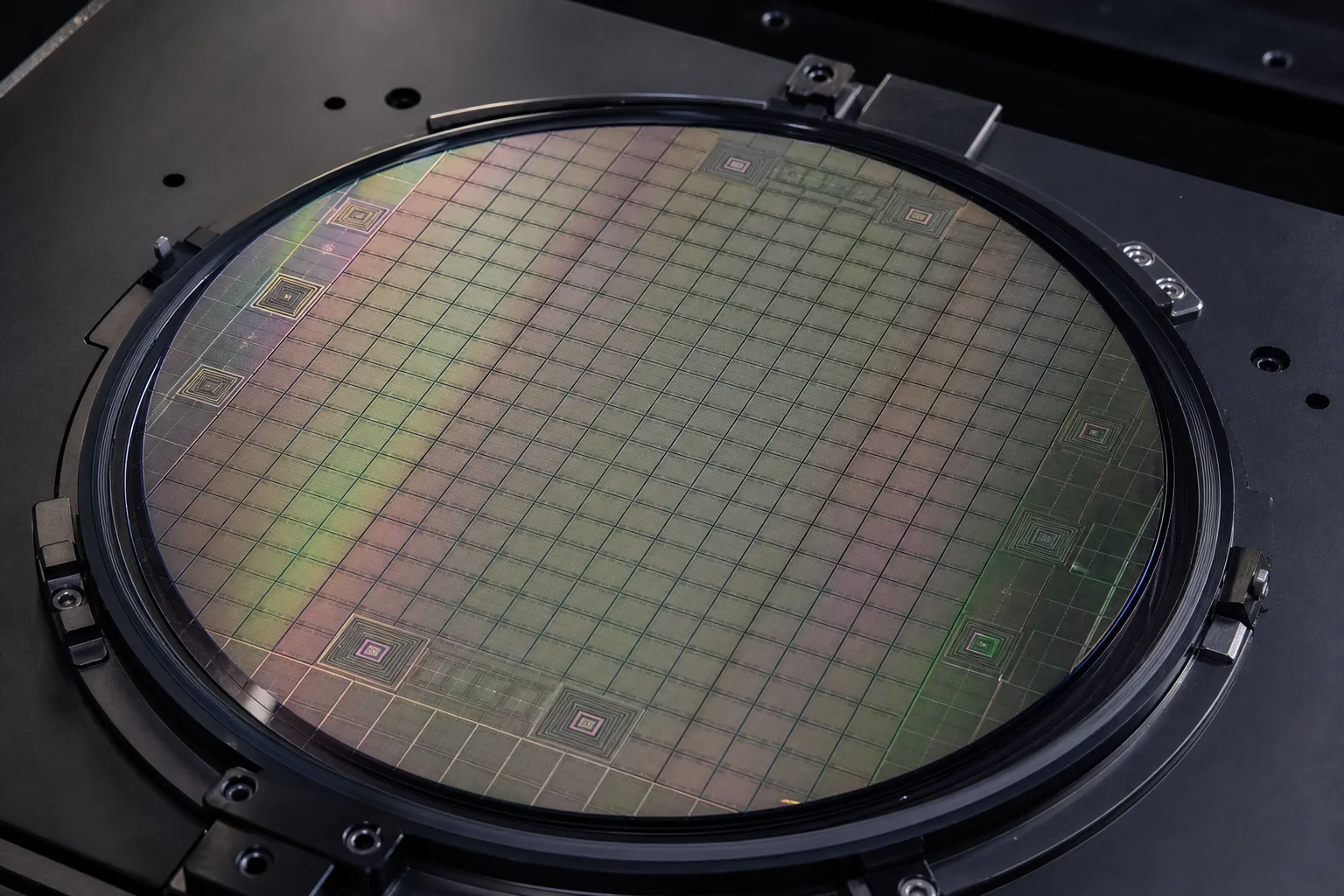
On-product overlay is still not a transistor width. It is a vector at each sampled point: how far this layer is from the corresponding point on the prior layer, in X and in Y. A single-machine overlay number is a tool capability. A matched-machine number is what happens when layer N and layer N+1 did not share a scanner. Film stress, polish, and damaged marks sit on top of the tool residual. None of those adders is a CD.
The wafer does not announce which number you are looking at. A patterned disk on a chuck is a picture of silicon. The traveler says whether the last visit was a CD recipe or an overlay recipe. Treating a scanner overlay in nanometers as proof of a transistor width is the same error as treating oxide color as proof of a node name.
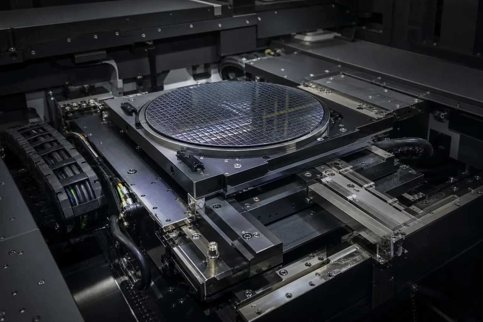
Read CD as a size. Read overlay as a registration. When a slide quotes a scanner overlay in nanometers, the open question is which layers, which machines, and whether the number is a tool residual or an on-product result. It is not asking how wide the transistor is.